
There are more than 720 species of carnivorous plants spread over 17 genera in 5 orders. This includes plants that are fully aquatic to ones that live in deserts, plants that live in rain forests, fog forests, temperate forests, bogs, fens, swamps, grasslands, lakes, streams, and on and on. There is no one way to grow carnivorous plants in general and no one way to grow any given carnivorous plant.
This Grow Carnivorous Plants section will help you grow and enjoy the more common and easier to grow carnivorous plants.
Growing Environments
General information on where to grow carnivorous plants. With a little ingenuity you can have a house and back yard full of carnivorous plants.
Growing Guides
Specific instructions on growing particular types of carnivorous plants. Try to concentrate on growing plants you can grow.
Propagation
How to make new plants. Propagating plants is fun.
Soils, Water, Light
The basics of a plant's life.
Feeding Plants
Plants need food too. Most carnivores need to be fed if there is no food for them to catch.
Pests & Other Issues
Carnivorous plants have enemies and diseases just like every other plant.
There are other nuggets of growing information scattered throughout the ICPS web site and its associated sites.
- ICPS FAQ (Frequently Asked Questions) -- Barry Rice's sometimes irreverent attempt to answer all your questions.
- Carnivorous Plant Newsletter index -- Find and read articles in old issues of CPN.
- ICPS Facebook forum -- The forum is essentially inactive but the information from old posts is invaluable.
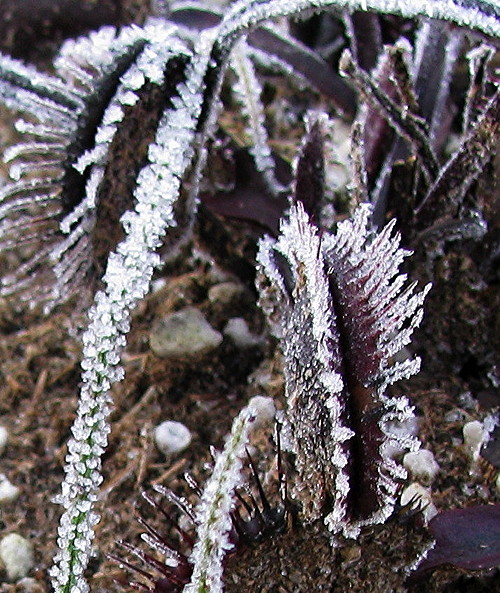
Hoar Frost on Venus Flytrap is no big deal. Photo by Djoni Crawford.